
File:Cmos-chip structure in 2000s (en).svg

Commons is a freely licensed media file repository. You can help.
Summary
| Description |
Català: Estructura esquemàtica d'un xip CMOS, tal com es va construir a principis dels anys 2000. El gràfic mostra els LDD-MISFET sobre un substrat de silici SOI amb cinc capes de metal·lització i un tap de soldadura per a la unió de xip. També mostra la secció per a FEOL (front-end de línia), BEOL (back-end de línia) i les primeres parts del procés de back-end. (versió traduïda a l'alemany)
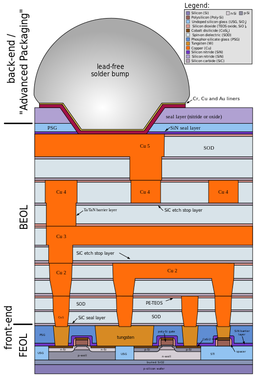
English: Schematic structure of a CMOS chip, like it is built in the early 2000s. The graphic shows LDD-MISFET's on a SOI silicon substrate with five metallization layers and solder bump for flip-chip bonding. Also it shows the section for FEOL (front-end of line), BEOL (back-end of line) and first parts of back-end process. Self made from university scripts and scientific papers |
||
| Date | |||
| Source | Own work | ||
| Author | Cepheiden | ||
| Other versions |
File:Cmos-chip structure in 2000s (en).svg contains 2 translations.
|
||
| SVG development |
|
.svg&lang=ca)
.svg&lang=en)

.svg)
.svg)
Licensing

|
Permission is granted to copy, distribute and/or modify this document under the terms of the GNU Free Documentation License, Version 1.2 or any later version published by the Free Software Foundation; with no Invariant Sections, no Front-Cover Texts, and no Back-Cover Texts. A copy of the license is included in the section entitled GNU Free Documentation License. |
| This file is licensed under the Creative Commons Attribution-Share Alike 3.0 Unported license. | ||
Attribution:
Cepheiden | ||
| ||
| This licensing tag was added to this file as part of the GFDL licensing update. |
- You are free:
- to share – to copy, distribute and transmit the work
- to remix – to adapt the work
- Under the following conditions:
- attribution – You must give appropriate credit, provide a link to the license, and indicate if changes were made. You may do so in any reasonable manner, but not in any way that suggests the licensor endorses you or your use.
File history
Click on a date/time to view the file as it appeared at that time.
| Date/Time | Thumbnail | Dimensions | User | Comment | |
|---|---|---|---|---|---|
| current | 14:35, 5 February 2024 | | 550 × 810 (138 KB) | Manlleus | File uploaded using svgtranslate tool (https://svgtranslate.toolforge.org/). Added translation for ca. |
| 14:25, 5 February 2024 |  | 550 × 810 (97 KB) | Manlleus | fixed text labels for translation | |
| 18:52, 9 December 2006 |  | 550 × 810 (85 KB) | Cepheiden | {{Information |Description= Schematic structure of a CMOS chip, like it is build in the early 2000s. The grafic shows LDD-MISFET's on a SOI silicon substrate with five metallization layers and solder bump for flip-chip bonding. Also it shows the section f | |
| 18:49, 9 December 2006 |  | 550 × 810 (85 KB) | Cepheiden | {{Information |Description= Schematic structure of a CMOS chip, like it is build in the early 2000s. The grafic shows LDD-MISFET's on a SOI silicon substrate with five metallization layers and solder bumb for flip-chip bonding. Also it shows the section f |
File usage
The following 4 pages use this file:
Global file usage
The following other wikis use this file:
- Usage on ca.wikipedia.org
- Usage on fa.wikipedia.org
- Usage on fi.wikipedia.org
- Usage on hy.wikipedia.org
- Usage on id.wikipedia.org
- Usage on ja.wikipedia.org
- Usage on ko.wikipedia.org
- Usage on zh.wikipedia.org
.svg?lang=en)